- Metrology - Laboratory
- Metrology and Test Equipment
- Critical dimension measuring system
- TZTEK Technology Co.,ltd
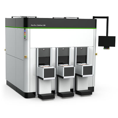
Critical dimension measuring system DaVinciopticalfor wafersnon-contact
Add to favorites
Compare this product
Characteristics
- Measured physical value
- critical dimension
- Technology
- optical
- Measured material
- for wafers
- Other characteristics
- non-contact, high-precision, high-speed, non-destructive
Description
Overlay
Overlay is a process to align the upper layer with the lower layer. The overlay error is defined as the deviation between these two layers. Overlay error measurement is an imaging process of calculating the deviation on two different overlay marks which mostly are generated by different processes and composed of different materials.
For Overlay measurement, Box-in-Box, Frame-in-Frame, L-Bars, Circle-in-Circle, Cross-in-Cross or customized structures are supported.
Critical Dimension
Optical measurement is a non-contact, non-destructive measurement technique and it is precise and fast. The structure width can be calculated by extracting intensity information from images. The intensity images should be processed to prevent it from interference by noise or deformation.
TZTEK’s metrology system provides the function to eliminate such interference. For structure width which is less than 0.7 μm, UV light can be applied.
Film Thickness
The system is designed to measure thickness of transparent or semitransparent dielectric film(resist) up to three layers. The automatic calibration function is integrated.
main features
•Measurement of critical dimensions, overlay
•Customization available for OC, SMIF and FOUP
•Available for wafer size 200/300 mm and the combination
•Visible light and UV light are optional
•SECS/GEM
Related Searches
- Measuring machine
- Optical measuring machine
- Automatic measuring machine
- High-precision measuring machine
- Measuring system for industrial applications
- Parts measuring machine
- Distance measuring machine
- Non-contact measuring machine
- Diameter measuring machine
- Video measuring machine
- Thickness measurement system
- CNC measuring machine
- High-speed measuring machine
- Contour measuring machine
- Angle measuring machine
- Shape measuring machine
- High-resolution measuring machine
- Roundness measuring machine
- Wafer measurement system
- Concentricity measuring machine
*Prices are pre-tax. They exclude delivery charges and customs duties and do not include additional charges for installation or activation options. Prices are indicative only and may vary by country, with changes to the cost of raw materials and exchange rates.


