- Materials - Tools - Components
- Semi-finished products
- Ceramic substrate
- Xiamen Innovacera Advanced Materials Co., Ltd
- Company
- Products
- Catalogs
- Projects
- News & Trends
- Exhibitions
Substrate for the electronics industry aluminum oxidethick-filmthin-layer

Add to favorites
Compare this product
Characteristics
- Options
- aluminum oxide, for the electronics industry
- Type
- thick-film, thin-layer
Description
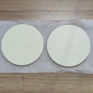
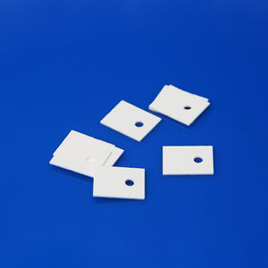
Alumina Oxide is one of the most cost-effective and widely used substrate materials in microelectronic applications. While many customers will be satisfied with an as-fired surface for their applications, there are four major benefits of ceramic substrate polishing:
Finer Line Patterns
After the fine grinding and polishing process, the ceramic substrate can get finer pattern lines, which is beneficial to the denser circuit design ability and is conducive to fine-pitch, high-density interconnection circuits.
An as-fired surface finish is generally adequate for lines as thin as 1 mil in thin-film applications and 5 mils in thick-film applications. Forming finer lines than these on as-fired surfaces will exhibit poor pattern definition resulting in increased conductor resistance, which inhibits current flow and reduces circuit performance. Poor pattern definition can also contribute to performance anomalies in RF and microwave circuits, so we will polish it.
Better Top and Bottom Surface Parallelism
Grinding and polishing the substrate can improves the parallelism between the top and bottom surfaces. The benefit is that the capacitance and inductance of the substrate can be more tightly controlled when the substrate is metalized and patterned. Since capacitance and inductance are the main factors determining impedance, increased parallelism can improve the predictability and performance of RF and microwave circuits.
VIDEO
Catalogs
No catalogs are available for this product.
See all of Xiamen Innovacera Advanced Materials Co., Ltd‘s catalogsOther Xiamen Innovacera Advanced Materials Co., Ltd products
Alumina Ceramic
Related Searches
- Ceramic
- Insulation ceramic
- Alumina ceramic
- Ceramic plate
- Tubular ceramic
- Substrate
- Ceramic rod
- High-temperature ceramic
- Protective ceramic
- Ceramic sheet
- Boron nitride ceramic
- Substrate for the electronics industry
- Ceramic substrate
- Silicon nitride ceramic
- Ceramic stick
- Tile ceramic
- Thermal pad
- Ceramic pipe
- Ceramic pad
*Prices are pre-tax. They exclude delivery charges and customs duties and do not include additional charges for installation or activation options. Prices are indicative only and may vary by country, with changes to the cost of raw materials and exchange rates.


