- Metrology - Laboratory
- Laboratory Equipment
- Electron microscope
- ZEISS Métrologie et Microscopie Industrielle
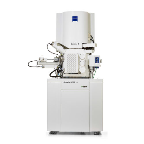
Field emission scanning electron microscope ZEISS GeminiSEM for researchindustrialhigh-contrast

Add to favorites
Compare this product
Characteristics
- Type
- field emission scanning electron
- Technical applications
- for research, industrial
- Other characteristics
- for detection, high-contrast
- Resolution
0.7 nm, 1.2 nm
Description
ZEISS GeminiSEM stands for effortless imaging with sub-nanometer resolution. These FE-SEMs (field emission scanning electron microscope) combine excellence in imaging and analytics. Innovations in electron optics and a new chamber design let you benefit from better image quality, usability and flexibility. Take sub-nanometer images below 1 kV without an immersion lens. Discover three unique designs of the ZEISS Gemini electron optics.
Ideal for core facilities - ZEISS GeminiSEM 360
Enabling efficient analysis - ZEISS GeminiSEM 460
New standard for surface imaging – ZEISS GeminiSEM 560
Benefit from surface sensitive imaging and gather information at low voltage or at high probe current. Discover the advantages of Inlens detection, NanoVP, contextual image viewing or AI-powered segmentation.
Switch seamlessly from low current-low kV work to high current-high kV work. Extend your possibilities with an in situ heating and tensile lab. Take advantage of a coplanar EDS/EBSD configuration, shadow-free mappings of EDS data and rapidly collecting EBSD maps with 4000 patterns/s.
Explore the new standard for surface imaging: magnetic field-free imaging with sub 1 nm resolution below 1kV without sample biasing or monochromation, Gemini 3 with its new electron optical engine Smart Autopilot, finding the sweet spot in your working conditions – and much more.
VIDEO
Catalogs
No catalogs are available for this product.
See all of ZEISS Métrologie et Microscopie Industrielle‘s catalogsOther ZEISS Métrologie et Microscopie Industrielle products
Industrial Microscopy
Related Searches
- Carl Zeiss microscope
- Carl Zeiss optical microscope
- Carl Zeiss laboratory microscope
- Inspection microscope
- Tabletop microscope
- LED illumination microscope
- Measuring microscope
- Polarization microscope
- Carl Zeiss analysis microscope
- Stereo microscope
- Upright microscope
- Bright field microscope
- Optical stereo microscope
- Carl Zeiss high-resolution microscope
- Industrial microscope
- Automatic microscope
- Metallurgical microscope
- Zoom stereo microscope
- Materials research microscope
- Fluorescence microscope
*Prices are pre-tax. They exclude delivery charges and customs duties and do not include additional charges for installation or activation options. Prices are indicative only and may vary by country, with changes to the cost of raw materials and exchange rates.


