- Products
- Interconnect
- Zhen Ding Tech. Group

- Products
- Catalogs
- News & Trends
- Exhibitions
Interconnect HDI
Add to favorites
Compare this product
Description
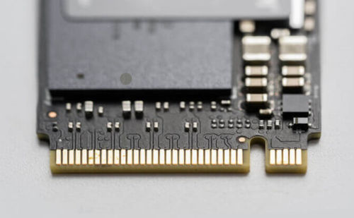
High Density Interconnect PCB. HDI has small size, high circuit distribution density, and good transmission efficiency, conducive to the use of advanced packaging technology, the cost is lower than traditional PCB when the layers exceeds 8L.
Small, high-density circuit distribution and high transmission efficiency.
The design of blind holes and buried holes makes the product occupy a small space, which is in line with the trend of light, thin, miniaturized of mobile electronic equipment.
Variety of stacks, diverse selection of raw materials, development towards high-end multilayer and Anylayer.
*Prices are pre-tax. They exclude delivery charges and customs duties and do not include additional charges for installation or activation options. Prices are indicative only and may vary by country, with changes to the cost of raw materials and exchange rates.


