- Electricity - Electronics
- Electronic Component
- zoolied inc.
- Company
- Products
- Catalogs
- News & Trends
- Exhibitions
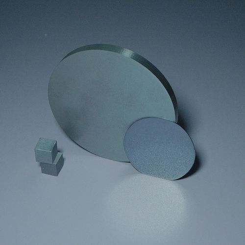
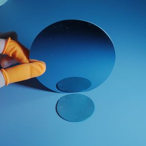
3 inch (75 mm) silicon wafer ZLY315
Add to favorites
Compare this product
Characteristics
- Other characteristic
- 3 inch (75 mm)
Description
Semiconductors are the core of electronic products, the cornerstone of the information industry, and are also known as the "food" of modern industry. But how much do we know about Silicon Wafers, the core material for making semiconductors? What is silicon wafers? Silicon wafer is the basic material for making semiconductor chips, it is the second most common element in the earth's crust, accounting for about 26%, second only to oxygen (49%). Silicon is widely present in high-concentration sand, gravel and rocks in the form of quartz (silica) in nature. Then through a series of complex processes such as purification and processing, it becomes the basic raw material-silicon wafer that meets the requirements of producing integrated circuits.
The production of silicon wafer usually has the following steps:
1) long crystal, which can be divided into CZ and FZ, because the fused polycrystalline material will directly contact with the quartz crucible, so the impurities in the quartz crucible will contaminate the fused polycrystalline. The CZ method is suitable for drawing large-diameter (300 mm) silicon wafers, which is the main Semiconductor Silicon Wafer material at present. As the polycrystalline raw materials are not in contact with the quartz crucible, there are few internal defects and low carbon and oxygen content, but the price is expensive and the cost is high. It is suitable for high-power devices and some high-end products.
2) slicing and drawing of the single crystal silicon rod need to cut off the head and tail material, then roll and grind it to the required diameter, cut the flat edge or V groove, and then cut into thin silicon wafer.
Catalogs
No catalogs are available for this product.
See all of zoolied inc.‘s catalogs*Prices are pre-tax. They exclude delivery charges and customs duties and do not include additional charges for installation or activation options. Prices are indicative only and may vary by country, with changes to the cost of raw materials and exchange rates.


